When Classical Spreading-Resistance Approximations Fail in Ultrathin Films
The familiar diffusive 1/a scaling is a limiting case, not a universal rule, in thin or laterally confined devices.
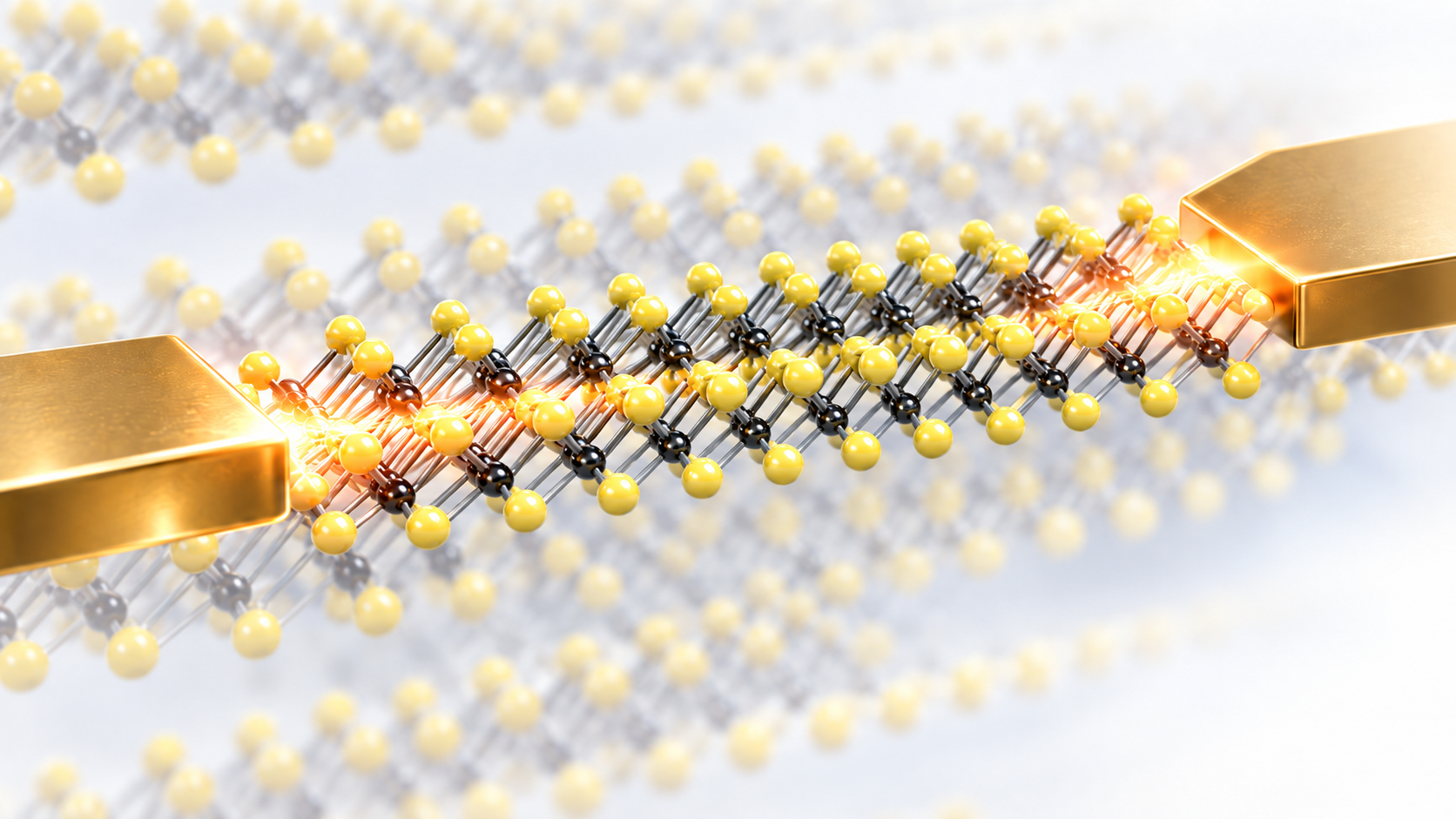
A famous (1/a) law with hidden assumptions
One of the most familiar results in spreading-resistance theory is the inverse-radius scaling
\[R_s \propto \frac{1}{a}.\]For a sufficiently large diffusive medium, this behavior is physically intuitive: a larger contact gives current more area through which to enter the material, so the constriction resistance decreases.
In anisotropic layered materials, a commonly used form replaces the bulk resistivity by an effective value and writes
\[R_s \approx \frac{\rho_{\mathrm{eff}}}{4a}.\]Our 2026 study shows that this expression remains useful — but only as a limiting case. When films become thin or laterally confined, the same formula can fail even if the experimental data look approximately linear over a narrow range.
When the classical limit works
The exact anisotropic solution was benchmarked against spreading-resistance measurements on highly oriented pyrolytic graphite.
In those measurements, the contact radii ranged from roughly 100 to 500 nm, while the graphite flake had a lateral extent much larger than the contact and a substrate thickness of about 2 mm.
This is close to the wide-and-thick asymptotic regime:
\[b\gg a, \qquad h_2 \text{ large}.\]Under those conditions, both the experimental trend and the exact anisotropic model recover the apparent (1/a) behavior.
For graphite, the measured anisotropy ratio used in the comparison was approximately
\[\alpha_2 \approx 2.73\times10^{-5},\]which is extremely anisotropic. Yet the classical scaling still emerges because the surrounding geometry is large enough to let the current spread toward its asymptotic pattern.
What changes when the device becomes finite
The agreement does not survive arbitrary scaling.
When the surrounding lateral dimension $b$ approaches the contact dimension $a$, current can no longer spread as if the material were infinite. The device boundary begins to reshape the field.
The paper shows that deviations become pronounced as (b/a) is reduced, with strong finite-boundary effects appearing below the wide-device regime. The conclusion section emphasizes that once (b/a) falls below roughly 20, or the film becomes only a few nanometers thick, the simple diffusive approximation can no longer be trusted.
At large (b/a), the resistance eventually saturates with increasing lateral extent because the remote boundary has become irrelevant.
Thin films introduce another constraint
Thickness matters for the same reason.
In a very thin lower layer, the current cannot penetrate deeply before encountering the bottom boundary. The spreading pattern becomes more two-dimensional and remains sensitive to the lateral geometry.
The MoS$_2$ benchmark illustrates this clearly. For a moderately anisotropic multilayer device with $b/a\approx20$ and $h_2=120~\mathrm{nm}$, the data can still display an apparent (1/a) dependence.
But if the lateral extent is reduced to about $b=5a$, or the thickness is reduced to only a few layers, such as $h_2=7~\mathrm{nm}$ in the model comparison, the exact solution departs substantially from the classical line.
Why an effective isotropic resistivity is not enough
A tempting workaround is to replace the anisotropic material by an effective scalar resistivity, for example using a geometric mean of the in-plane and out-of-plane components.
That may reproduce the classical asymptote but does not reproduce the finite-device field.
The paper demonstrates cases where the isotropic model fails to match the exact anisotropic result even when the same nominal effective resistivity is used.
The problem is structural: anisotropy changes the direction of current flow. A scalar replacement cannot reproduce that directional redistribution once boundaries become important.
The danger for parameter extraction
This matters because spreading-resistance measurements are often used to infer intrinsic material properties.
If a finite ultrathin device is fit with
\[R_s=\frac{\rho_{\mathrm{eff}}}{4a},\]the fitted $\rho_{\mathrm{eff}}$ can absorb geometry effects that do not belong to the material itself. Back-calculating in-plane or out-of-plane resistivity from that fit can therefore give a serious error.
The safer approach is to fit the resistance using the actual device dimensions and the full anisotropic field solution.
A useful way to remember the result
The classical (1/a) relation is not “wrong.”
It is the correct asymptotic result for a contact embedded in a sufficiently wide and thick medium.
The mistake is treating that asymptote as a universal contact law.
As devices move toward ultrathin layers, short channels and strongly anisotropic materials, the geometry stops being a small correction and becomes part of the physics that determines the measured resistance.