Why Anisotropic Conductivity Changes Current Crowding in 2D Thin Films
Layered materials conduct very differently in-plane and out-of-plane, reshaping current injection beneath vertical contacts.
Why current refuses to travel straight down
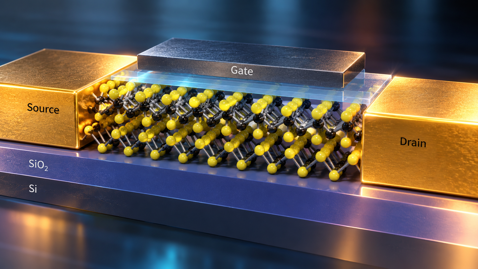
A vertical metal contact seems geometrically simple: current enters through the electrode and should flow downward into the semiconductor. That intuition works reasonably well for isotropic bulk materials. It becomes misleading in layered two-dimensional materials, where electrical conductivity can differ by orders of magnitude between the crystal plane and the out-of-plane direction.
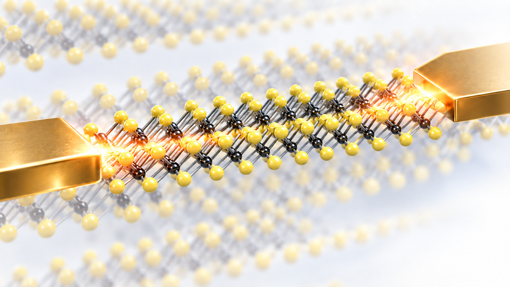
In materials such as graphite, MoS$_2$, and WSe$_2$, carriers move far more easily along the atomic layers than across them. The underlying crystal structure explains why. Strong in-plane bonding supports efficient lateral transport, while the weak van der Waals coupling between layers makes vertical motion comparatively difficult.
When a metal electrode is placed on such a material, the injected current therefore takes a path of lower resistance: it spreads laterally beneath the contact before penetrating downward.
That redistribution is the origin of strong current crowding near contact edges.
Anisotropy changes the field itself
The electrostatic problem is governed by the conductivity tensor,
$ \nabla\cdot\left(\boldsymbol{\sigma}\nabla\Phi\right)=0. $
For a layered medium, the in-plane and out-of-plane conductivities are different. Equivalently, the resistivity tensor contains distinct lateral and vertical components.
The paper defines anisotropy ratios such as
\[\alpha = \frac{\rho_{\parallel}}{\rho_{\perp}},\]so a small $\alpha$ corresponds to much easier in-plane conduction.
As $\alpha$ decreases, the potential distribution stretches laterally. Rather than dropping rapidly through the thickness, the potential remains correlated over a longer distance along the plane. The current-density pattern follows that field structure.
The consequence is subtle: stronger in-plane conductivity can reduce the overall spreading resistance while simultaneously increasing the localization of current near the contact perimeter.
Those are not contradictory results. One describes the total voltage drop; the other describes where the current is concentrated.
Why edge crowding matters
Current crowding is not only an electrical-resistance problem.
A highly localized current density produces localized Joule heating. In real contacts, this can accelerate electromigration, interfacial degradation, and thermally activated failure. A contact can therefore have an acceptable terminal resistance while still containing microscopic regions that carry much larger current density than the average value suggests.
For atomically thin and layered materials, this distinction becomes especially important because the geometric dimensions are already comparable to the characteristic current-spreading length scales.
A model that captures only terminal resistance may miss the spatial physics that controls reliability.
The top and bottom layers both matter
The exact framework in the paper treats both members of the vertical contact as anisotropic materials. Each layer has independent in-plane and out-of-plane resistivity, and the interface can have a finite specific resistivity $\rho_i$.
This is more general than treating a metal electrode as perfectly equipotential or replacing the semiconductor by a single effective resistivity.
The calculations show that for a fixed out-of-plane resistivity, lowering the in-plane resistivity increases lateral current spreading and sharpens the edge crowding. At the same time, the dominant lever for reducing total spreading resistance in a vertical contact is often the out-of-plane resistivity of the lower layer rather than pushing the in-plane resistivity lower and lower.
That distinction has an important design implication: a material can be extremely conductive laterally and still remain difficult to contact vertically.
Why isotropic intuition can fail
A common shortcut is to replace an anisotropic material with an effective isotropic resistivity. That may reproduce one limiting resistance value, but it cannot reproduce the actual field distribution in a finite device.
The paper shows that isotropic models fail particularly when lateral boundaries, thin-film thickness and strong anisotropy all matter at once.
This is why the full tensor treatment is useful. It predicts not only the total spreading resistance but also how the potential and current redistribute throughout the layered structure.
From contact optimization to reliability
The contact-design message is therefore broader than “reduce contact resistance.”
A robust vertical contact should minimize the total resistance and avoid unnecessarily severe current localization. Lowering interfacial resistivity remains important, but material anisotropy and geometry determine how the injected current reaches the channel after crossing the interface.
For highly anisotropic 2D materials, the current path is inherently nonlocal. The electrode edge, film thickness, lateral extent, and vertical resistivity all participate in the final electrical behavior.
That is why current crowding in layered contacts is fundamentally a field-distribution problem, not just a lumped-resistance problem.