Analytical Theory vs FEM for Anisotropic Vertical Contacts
How exact field theory, finite-element simulations, and published measurements converge on the same contact physics.
Why solve the same contact two different ways?
Analytical theory and finite-element simulation are sometimes presented as competing approaches. For electrical contacts in anisotropic thin films, they are more useful when treated as complementary tools.
An exact field solution exposes scaling and limiting behavior. FEM provides direct spatial visualization and can be extended to geometries that become cumbersome analytically.
In our anisotropic-contact study, we used both to test whether the same physical model produced the same resistance and current-crowding behavior.
The analytical side
The theory begins with the conductivity-tensor form of Laplace’s equation,
$ \nabla\cdot\left(\boldsymbol{\sigma}\nabla\Phi\right)=0. $
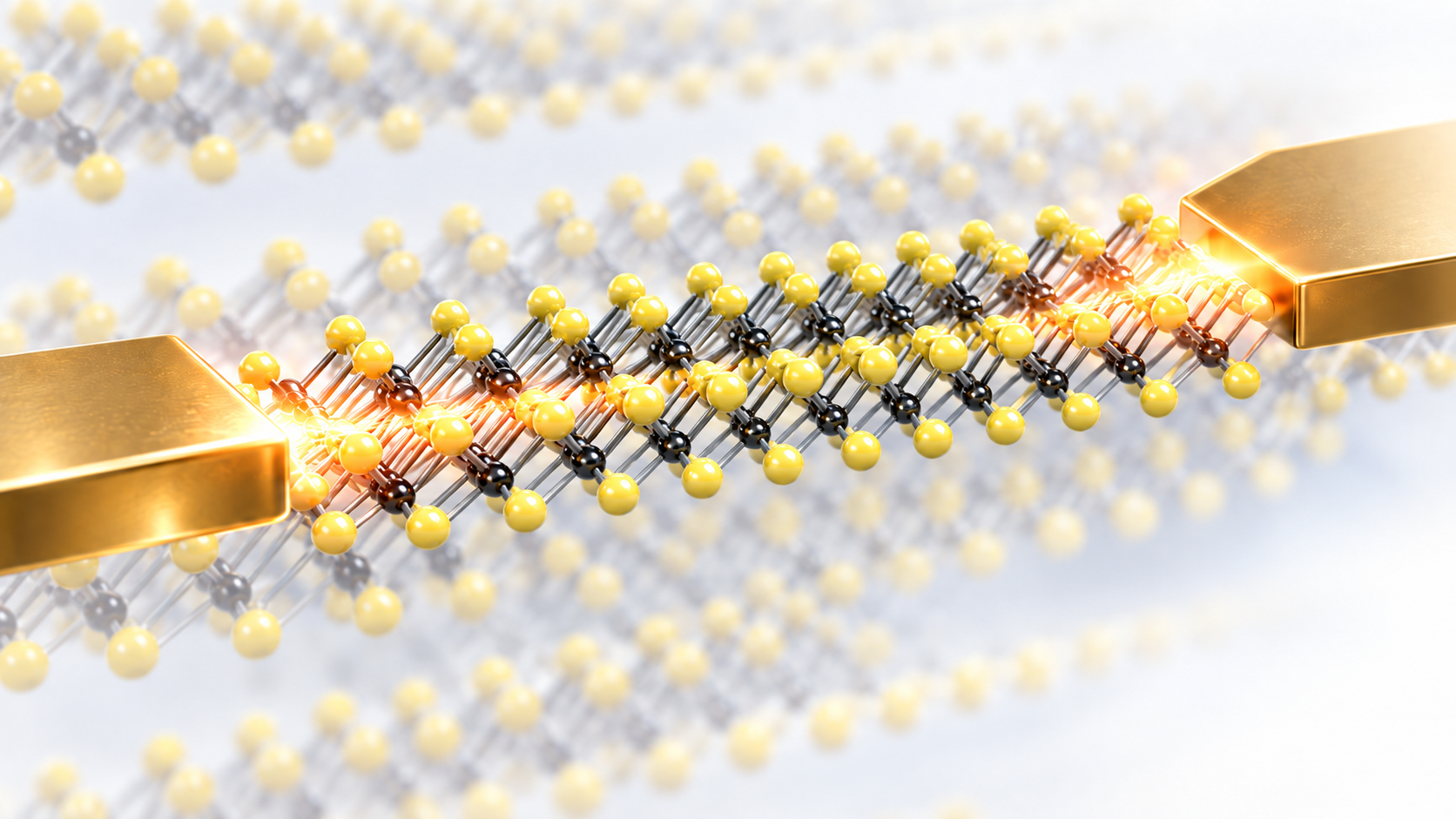
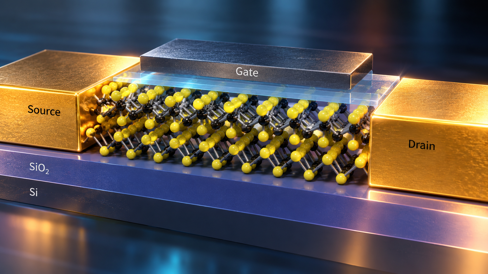
Both the top and bottom layers can be anisotropic, each with independent in-plane and out-of-plane resistivities. A finite specific interface resistivity $\rho_i$ is included, and finite lateral and vertical boundaries are retained.
Exact field expansions are derived for Cartesian contacts and cylindrical disk contacts.
From the potential, the current density follows from
\[\mathbf{J}=-\boldsymbol{\sigma}\nabla\Phi.\]This provides both the total resistance and the full spatial distribution of current.
The FEM side
The same geometry and material tensors were then implemented numerically in COMSOL.
FEM does not require the field to be expressed as a closed analytical series. Instead, the domain is discretized and the anisotropic conduction equation is solved directly.
That makes it particularly good for plotting equipotential contours and current-density maps. The edge crowding caused by high in-plane conductivity becomes visually obvious: potential spreads laterally beneath the contact, while current injection becomes increasingly concentrated near the perimeter.
Agreement is more valuable than either method alone
Across the parameter sweeps reported in the paper, the exact analytical results and FEM calculations show excellent agreement.
That agreement matters for two reasons.
First, it validates the algebra and boundary treatment of the analytical solution.
Second, it validates the numerical implementation against a solution that does not depend on mesh refinement or solver configuration in the same way.
When two mathematically independent routes converge, confidence in the physical result is much stronger.
Experimental benchmarks add a third layer
The study also compares the theory with published measurements on graphite and multilayer MoS$_2$.
For highly oriented pyrolytic graphite, the experimental contact sizes and thick substrate place the system close to the classical wide-and-thick limit. The exact anisotropic solution reproduces the observed inverse-radius trend using the measured anisotropy, without introducing fitting parameters to force agreement.
For multilayer MoS$_2$, the same framework captures the regime where the classical diffusive model works and predicts where it will fail as the film becomes thinner or the lateral extent becomes smaller.
This three-way comparison — analytical theory, FEM, and experiment — is stronger than validating one numerical model against another.
What each method is best at
The analytical solution is ideal for:
- rapid parameter sweeps;
- identifying asymptotic scaling;
- isolating the role of anisotropy;
- fitting experimental data efficiently;
- serving as a reference solution for numerical codes.
FEM is ideal for:
- visualizing local current density and potential;
- adding geometric details;
- treating nonuniform interfaces;
- exploring device shapes outside the separable analytical geometries.
The two approaches therefore serve different stages of the same design workflow.
No-fitting-parameter validation is important
One particularly useful feature of the experimental comparison is that the model does not need an arbitrary fitting factor to recover the reported graphite and MoS$_2$ trends.
That makes the comparison a test of the physical field formulation rather than merely a curve-fitting exercise.
It also helps reveal why a simpler isotropic effective-medium model may appear adequate in one geometry and fail badly in another. The full theory knows the actual device width, film thickness and conductivity tensor, so it can distinguish a true material effect from a finite-geometry effect.
A broader modeling lesson
For nanoscale electronic devices, numerical simulation is increasingly easy to run. That convenience can make it tempting to treat the numerical output as the final answer.
The contact problem illustrates why an analytical reference remains valuable.
A field solution tells us why a trend occurs, which parameters control it, and what happens in limiting cases. FEM then provides the flexibility to move beyond the idealized geometry without losing that physical intuition.
The strongest model is therefore not necessarily the most computationally elaborate one. It is the one that can be checked from multiple independent directions.